)
)
Microelectronics UK 2026 Startup Spotlight: Hybrid Integration

In the latest in a series inviting innovative startups to tell their stories, Microelectronics UK features Hybrid Integration, a provider of advanced microelectronic and photonic packaging across technical project delivery, targeted support and failure analysis. The company was founded in 2025 and has more than 40 years of combined industry experience, and its leadership team comprises CTO and founder Dr Chris Lewins and COO David Kane.
You can find out more about Hybrid Integration here. Many thanks to Dani Parsons for helping provide these answers.
---
In one sentence, what does your company do?
Hybrid Integration helps innovators turn photonic chips and chiplets into commercial products, providing flexible packaging, design and integration tailored to each project’s application and performance requirements.
How did the business come about?
Our founder, Chris, spent more than 10 years working in the photonics packaging industry at companies including EFFECT Photonics and Oxford Ionics. Throughout his career, he came up against the same challenges time and time again: packaging that either didn’t meet the technical requirements of the project, wasn’t accessible to SMEs, or was too slow or inflexible.
Existing suppliers often couldn’t provide the level of design, integration or flexibility his projects needed, so he found himself making compromises or just doing it himself – neither of which felt like a good option.
Chris created Hybrid Integration to address that gap and provide advanced packaging support for teams working at prototype and low-to-medium volumes, with support built around the needs of each project.

What industry problem are you solving?
We’re helping fill a gap in the UK advanced photonic packaging landscape by making high-performance, flexible packaging more accessible for SMEs and R&D teams.
Teams looking for low-volume production (under 1,000 units) are faced with three main options:
- Working with a small packaging house – who may rely on legacy techniques, fixed form factors and standardised processes.
- Building a packaging capability in-house – which requires significant investment, dedicated facilities and specialist knowledge.
- Sending their PICs overseas for packaging – which increases lead times and creates challenges for high-security projects.
The result is a gap in the market for flexible packaging support for smaller teams and lower-volume projects. We think people creating innovative technology should be able to access packaging that works around their needs, rather than having to adapt their product to fit what’s already available.
Why is this problem becoming more important right now?
This issue is becoming increasingly important as PICs become more and more complex. Traditional packaging approaches can limit both device performance and design flexibility, forcing designers to work around fixed form factors and making more advanced architectures, such as flip-chip, difficult or impossible to implement.
Going overseas is often not practical either, especially for the defence and aerospace sectors that have strict sovereignty requirements. So, teams are left trying to put their own packaging together – something that requires specialist expertise in-house.
The result is that many SMEs struggle to commercialise innovative technologies quickly enough to be competitive. Larger organisations can invest in in-house packaging capabilities or leverage established manufacturing partnerships, but smaller teams are often left compromising between performance, cost and delivery times.
As semiconductor and photonic technology continues to advance, this gap is becoming increasingly difficult to ignore.
What makes your approach different from existing solutions?
We’re motivated by making innovative solutions actually work outside of a lab environment, so we’re always looking for the packaging options that allow your product to perform in your chosen application.
We start by understanding the application, what you’re trying to achieve and the technical and commercial requirements of the project – and we help find the packaging approach that fits best. We can help you understand trade-offs and make informed decisions that support both device performance and delivery timescales.
We work at levels from individual dies to hundreds of units, making high-performing advanced packaging more accessible for prototyping, R&D and low-volume production – an underserved area in the UK.
What has been the biggest challenge in scaling the business so far?
Our biggest challenge has been scaling sustainably without external investment. We’re bootstrapped, so every investment we make has to be carefully considered. That means focusing on capabilities we know the market actually needs, all while balancing long-term growth with the everyday costs of running a business.
It’s a capital-intensive business, and the specialist equipment we need to deliver cutting-edge solutions can cost hundreds of thousands, so every purchase is a significant investment given our size. Add to that ever-growing staffing costs and our need for highly specialised expertise, and scaling becomes a real balancing act. It’s all part of the fun of running a startup, though!
What has been your biggest milestone to date?
Our biggest milestone has to be the purchase of our Nanoscribe two-photon polymerisation (2PP) 3D printer.
In simple terms, it allows us to manufacture nanoscale optical components – think tiny lenses and optical interconnects – quickly and with exceptionally high precision. This technique allows us to print things that are difficult or impossible to achieve through conventional manufacturing.
This technology is huge for us. It gives us much more freedom to create custom components around the specific needs of a project and expand our ability to support customers working at low volumes.
Importantly, nobody else offers this service commercially in the UK. The only comparable systems we know of are in big companies or academic institutions – so aren’t accessible to industry as a service.
It was a significant purchase for us, especially just over a year into business, but we really believe in the value this technology brings to the UK photonics ecosystem.
What excites you most about the future of the microelectronics industry?
We’re really excited to see how advanced packaging develops over the next few years. We’ve seen such huge progress in PIC technology, and we think advanced packaging is the natural next thing to follow.
We’re already seeing more government investment and growing industry demand, so we’re excited to see the new technologies and processes that emerge over the next few years.
We’re also keeping a close eye on quantum technologies – the UK is producing world-leading research and seeing some huge breakthroughs in the sector, and we can’t wait to see what opportunities this opens up for the country and the wider tech sector. It’s an exciting area to watch, and we’re looking forward to helping turn that innovation into real products.
What’s next for the business over the next 12 months?
Now we’ve got our 2PP 3D printer, we’re working hard on building that side of the business – from commissioning the system and developing manufacturing processes to engaging with customers.
The installation of the machine also marks the beginning of our engineering centre in Belfast, so we’ll be continuing to grow our presence in Northern Ireland alongside our current operations in Devon.
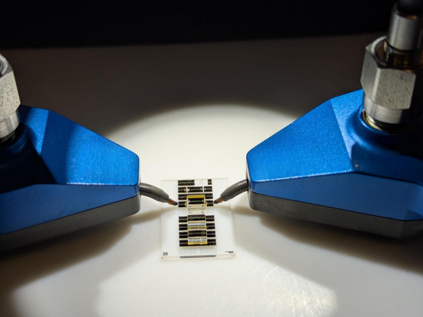
That’ll keep us busy for a while, but we’re also continuing development for Starpack – our reconfigurable advanced packaging platform. We're expanding its photonic integration capabilities to support multiple PICs within a single package with fast turnarounds.
Alongside the technical work, we'll be attending events across the UK (and a few internationally) to build awareness of what we're doing. If you’d like to meet the team, you can find us at Microelectronics UK, and we’ll be sharing details of our other events on LinkedIn throughout the year.