)
)
Microelectronics UK 2026: Q&A: Madhuparna Datta, Cadence
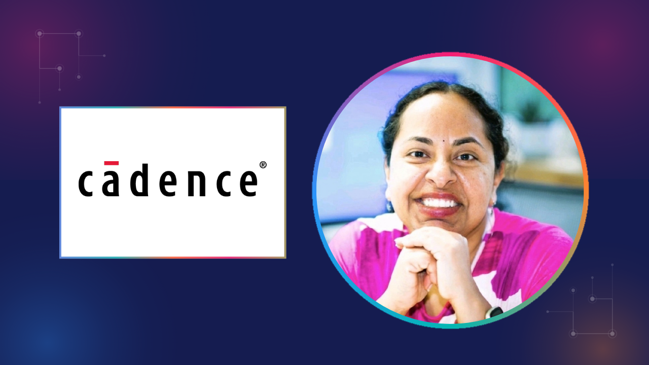
Ahead of Microelectronics UK, on September 29-30 at Excel London, Madhuparna Datta, application engineering director at Cadence, talks about her excitement for AI-driven engineering, chiplet-based architectures, and multi-physics design methodologies, as well as the challenge of data infrastructure for AI-driven engineering.
Tell us about your role at Cadence - what problems are you solving, and for whom?
I am an application engineering director at Cadence and lead people and technology with equal passion. I oversee digital and signoff technical campaigns across the region, working closely with customers on cutting-edge designs including CPUs, GPUs, and system IPs on the most advanced nodes (2nm, A14 etc). In my career span, I have worked across the full electronics stack, spanning silicon, packaging, and board-level design, helping customers transform innovative ideas into successful products.
What are the defining technical and operational pressures facing your sector right now - and where do you see the industry underestimating the challenge?
The defining pressure on the semiconductor sector today is managing complexity. The industry is moving from scaling individual chips to building heterogeneous systems that combine multiple dies, chiplets, advanced packaging, software, and AI workloads. At the same time, customers are demanding higher performance, lower power consumption, faster time-to-market, and greater reliability, particularly for AI infrastructure, communications, and automotive applications. Cadence has highlighted AI-driven silicon and systems, hyperscale computing, communications, automotives and life sciences as key growth areas driving this complexity.
Where I believe the industry is underestimating the challenge is in three areas. First and probably the most spoken about is data infrastructure for AI-driven engineering. AI is generating enormous excitement, but its effectiveness depends on high-quality, connected design data rather than fragmented legacy flows. Second, multi-physics engineering including thermal effects, power integrity, and mechanical stress are no longer late-stage verification problems but must be addressed much earlier in the design process, especially for 3D-ICs and chiplet-based systems. Finally, there is a significant skills challenge. Future semiconductor development requires engineers who can work across silicon design, packaging, physics, software, and AI, yet the industry is not developing this multidisciplinary talent fast enough. In my view, solving the skills gap may prove just as important as solving the technical challenges themselves. Encouragingly, initiatives such as the Novomorphic, UK's Student Talent Awards for semiconductors and the work of UKESF are helping to bridge that gap by raising awareness of the sector, nurturing emerging talent, and creating pathways into the industry for the next generation of engineers.
Which application areas or end markets present the strongest near-term opportunity for your technology, and what is driving that demand?
The strongest near-term opportunities are in AI infrastructure, hyperscale data centres, and automotive systems which are quite interconnected. The rapid growth of generative AI is driving unprecedented demand for advanced processors, high-bandwidth memory, chiplets, and energy-efficient system architectures, creating significant challenges in chip, package, and system design. The recent increase in memory prices and its impact on overall product cost well illustrates this point. At the same time, the automotive industry is undergoing a major transformation towards software-defined, electric, and autonomous vehicles, which require increasingly sophisticated semiconductors and system-level engineering in terms of physical AI. These markets are pushing the limits of performance, power efficiency, thermal management, and reliability, creating strong demand for Cadence's design, verification, multi-physics analysis, and AI-driven engineering solutions.
Which emerging technologies or engineering approaches are you backing for the next three to five years - and what would it take for them to cross from promising to mainstream?
Over the next three to five years, I am particularly excited about AI-driven engineering, chiplet-based architecture, and digital twins/multi-physics design methodologies. AI has the potential to dramatically improve engineering productivity and help teams explore far more design options than would be possible manually. Chiplets and advanced packaging are becoming essential as traditional scaling becomes increasingly challenging, enabling companies to combine the best technologies from different process nodes and suppliers into a single system. At the same time, digital twins and multi-physics analysis are becoming critical for understanding system behaviour, including power, thermal and mechanical effects, much earlier in the design cycle.
For these technologies to move from promising to mainstream, three things are needed. First, industry standards and interoperability must mature, particularly around chiplet ecosystems and heterogeneous integration. Second, organisations need trusted, connected data foundations so that AI-powered engineering tools can deliver consistent and repeatable results. Third, we need to continue investing in skills development, creating engineers who can work across silicon, packaging, software and systems disciplines. In many ways, the technology is advancing faster than the industry's ability to scale the expertise needed to deploy it effectively.
Events like Microelectronics UK bring together engineers, researchers, and industry decision-makers under one roof. How valuable is that kind of in-person concentration of expertise to you and your team?
Events like Microelectronics UK are incredibly valuable because they bring together people from across the semiconductor ecosystem who would not normally have the opportunity to interact in one place. Innovation in our industry depends on collaboration between manufacturers, design companies, tool providers, researchers, universities, startups, and government, and these events create a unique environment for sharing ideas, discussing common challenges, and building partnerships.
From my perspective, the greatest value comes from the conversations that happen between the presentations and at the evening networking reception. They help us understand emerging technology trends, identify skills and talent gaps, and learn how others are tackling similar engineering challenges. As the industry moves toward more complex systems involving AI, advanced packaging, and chiplet-based architectures, no single organisation can solve these challenges alone. Bringing together technical experts, researchers, policymakers, and business leaders helps accelerate innovation and ensures the UK remains competitive in a rapidly evolving global market.
These events are also important for inspiring the next generation of engineers. They provide a platform to showcase exciting technologies, connect students with industry leaders, and strengthen initiatives aimed at developing the diverse, multidisciplinary talent the sector will need in the years ahead.
What do you want engineers and technical buyers to come away understanding about Cadence after speaking with you at the show - and what conversations are you expecting to have on the floor?
I would like engineers and technical decision-makers to come away with the understanding that Cadence is helping enable the next generation of innovation, from AI infrastructure and advanced semiconductors to automotive, communications, and intelligent systems. We are no longer solving isolated chip design problems. We are helping customers tackle increasingly complex system-level challenges involving silicon, packaging, software, power, thermal management, and AI-driven design. Cadence's strategy is centred around engineering design for the AI era, combining design excellence, system innovation, and computational software to help customers bring breakthrough products to market faster.
The conversations I expect to have on the show floor will largely focus on how organisations are managing the growing complexity of advanced-node design, AI infrastructure, chiplet integration, 3D-ICs, and system-level optimisation. I expect many discussions around adopting AI in engineering workflows, improving productivity, addressing power and thermal challenges, and navigating the skills gap facing our industry. These conversations are valuable because they provide an opportunity to exchange experiences, understand emerging challenges, and explore how collaboration across the semiconductor ecosystem can accelerate innovation.
Ultimately, I would like people to see Cadence not just as a technology supplier, but as a trusted partner helping customers solve some of the industry's most difficult engineering challenges and enabling the innovations that will shape the next decade of computing, communications, transportation, and AI.
Is there a leader, engineer, or mentor who has shaped how you approach your work - and what is the most enduring lesson you took from them?
I have been fortunate to work with several outstanding leaders and mentors throughout my career, but the most enduring lesson I have taken from them is that technology alone is never enough. Success comes from understanding the problem you are trying to solve, listening carefully to customers and colleagues, and building strong teams that can work across disciplines. As the semiconductor industry becomes increasingly complex, the ability to bring together diverse expertise is often more important than individual technical brilliance.
Another lesson that has stayed with me is to remain curious and keep learning. The technologies, tools, and challenges we face today are very different from those I encountered at the start of my career. The best engineers and leaders are those who continually adapt, embrace new ideas, and remain open to different perspectives. That's an approach I have tried to carry forward in both my technical work and leadership style.
What does the next 12 months look like for Cadence - in terms of product direction, capability expansion, or where you are focusing development resource?
For the next 12 months, I see Cadence focusing on three key areas: AI-driven engineering, advanced system design, and supporting the AI infrastructure that is driving demand across the semiconductor industry. Cadence is investing heavily in applying AI to improve engineering productivity, helping design teams explore more options, optimize designs faster, and manage the growing complexity of modern semiconductor development. At the same time, there is a strong focus on enabling advanced architectures such as chiplets, 3D-ICs, and heterogeneous integration, which are becoming essential as traditional scaling approaches reach their limits.
From a customer perspective, much of the development effort will continue to centre on helping organisations design the next generation of AI, hyperscale computing, communications, and automotive systems. These applications are pushing the boundaries of performance, power efficiency, thermal management, and system integration, requiring a much more holistic approach that spans silicon, packaging, and system analysis. Cadence's strategy increasingly brings together design tools, AI, digital twins, and multi-physics analysis to address these challenges earlier in the design cycle.